

 SK hynix's 128-Layer 1Tb TLC NAND Flash")
SK Hynix today said it has begun mass producing the world’s first 128-layer NAND product and will kick off sales in the second half of the year.
A quick transition to 128-layer tech will give SK Hynix production cost and NAND density advantages over the competition. The Korean NAND fabber is currently ramping up sales and production of its 96-layer die technology, as are Intel, Micron, Samsung and Toshiba/Western Digital.
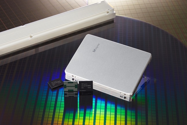
The 128-layer product is formatted as TLC (3bits/cell) and provides a 1Tb die. 128-layer NAND is one-third more dense than 96-layer alternatives.
Some competitors have 1Tb QLC (4bits/cell) die tech, but SK hynix said QLC represents less than 15 per cent of the market. According to the company TLC accounts for more than 85 per cent of the NAND market.
The SK hynix technology has logic at the base of the die with NAND cells stacked in layers above this. It says the 1Tb 128-layer die increases bit productivity per wafer by 40 per cent compared to its 96-Layer NAND.
It will develop a 1Tb UFS 3.1 product for mobile phone use, using 128-layer tech, halving the chips needed for 1TB of phone memory compared to 512Gb technology and needing 20 per cent less power.
In 2020 SK Hynix will develop 2TB consumer SSDs using this technology, and also 16TB and 32TB NVMe data centre SSDs.
SK hynix is also developing next-generation 176-Layer NAND as well, 48 layers more than 128, representing an approximate 30 per cent increase in density.


