


Western Digital and Toshiba have developed a 128-layer 3D NAND die with TLC (3bits/cell) cell formatting and 512Gbit capacity.
A 128-layer die will be BiCS-5 in Toshiba flash generation naming terminology – BiCS-4 is 96-layer and BiCS-3 is 64-layer.
Adding 32 more layers should add a third more capacity – assuming the same process technology is used as in the two companies’ 96-layer 3D NAND. Accordingly, flash drives built with 128-layer dies could have a third more capacity than 96-layer drives. Alternatively they could be built to the same capacity at reduced cost. Product might appear in late 2020, with production ramping in 2021.
Wafer-thick
Senior Wells Fargo analyst Aaron Rakers has built a production model that assumes 66mm2 die size and a 7.8Gb/mm2 bit density rating. He thinks WD-Toshiba has the industry’s highest NAND density and models the suppliers at an 85 per cent wafer yield:
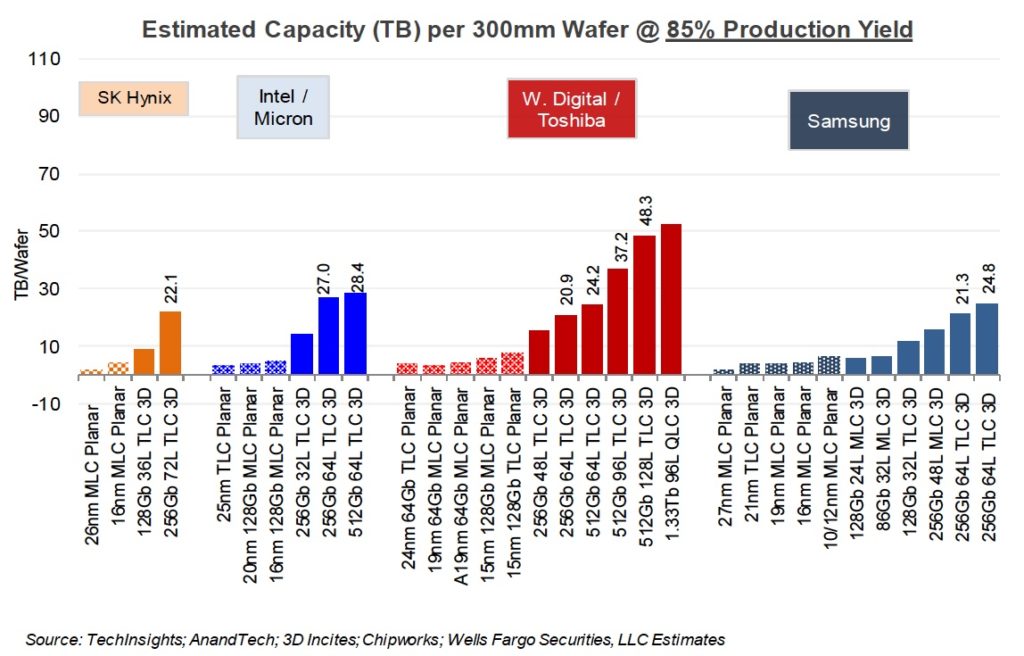
The die uses a Circuit-under-Array (CuA) design in which the logic circuits are built at the bottom of the chip with the data layers stacked above. Rakers says “his enables a 15 per cent smaller die size vs. non-CuA technology; we estimate a 23 per cent total die shrink vs. 96-layer.”
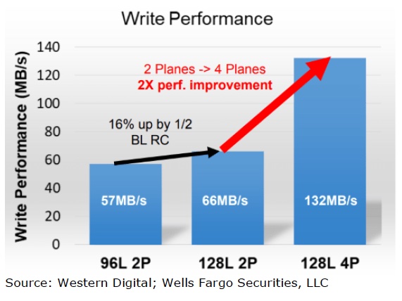
Partly through this freed-up space W. Digital was able to utilise four planes (vs. traditionally 2 planes) to increase performance by 2x. The die is divided into four planes or sections which be accessed independently and in parallel. Because of this it can reach a 132MB/sec program throughput level.
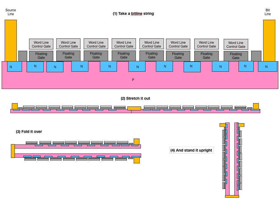
The chart refers to bitlines and their place in the NAND world is explained here.
The 132MB/sec speed exceeds the 83MB/sec program throughput of a 110+ layer chip from Samsung which can operate at 1.2Gbit/s IO bandwidth and has a 45 microsecond read time.
WD is accessing data on the 128-layer die using 4KB pages and not the industry standard 16KB pages which limits electricity usage.
Lastly, this is a TLC die. A QLC (4bits/cell) version would have a third more capacity again – 682Gbit.
WD presented this technology last month at the International Solid State Circuits Conference in San Francisco.


