


Toshiba has a new way to connect an SSD’s controller and flash chips, making higher-capacity and faster SSDs possible – at levels not yet seen.
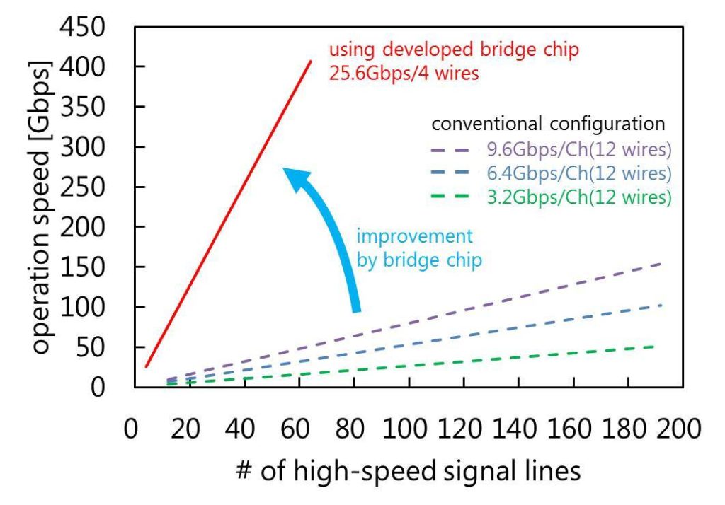
SSD capacities are limited by the number of connections between the controller and the flash chips. Currently high-speed signal lines connect the chips to the controller. The more chips there are the more signal lines are needed. But the SSD’s operating speed decreases as more chips are connected, thus limiting the SSD’s capacity.
It is even difficult to implement the wiring on the SSD board.
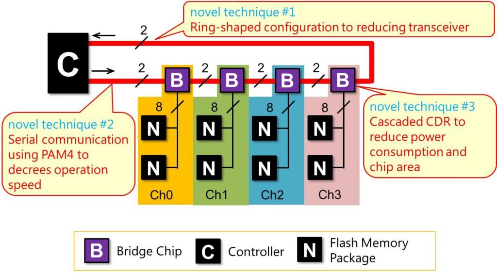
The answer is to insert a bridge chip between the controller and the flash chips. Toshiba’s bridge chip relies on a daisy chain connecting the controller and bridge chips in a ring shape. It uses a serial communication using PAM 4 (4-level Pulse Amplitude Modulation) and a jitter improvement technique for eliminating a Phase Locked Loop (PLL) circuit in the bridge chip.
A PLL circuit generates an accurate reference signal. Jitter is fluctuation in the time domain of the clock or signal waveforms which degrades signal recognition.
These three techniques reduce the size and power consumption of the bridge chip, making it possible to operate a larger number of flash memory chips at high speed with fewer high-speed signal lines.
Toshiba says it will further enhance bridge-chip performance while reducing the chip’s area and power consumption. Its aim is to achieve high-speed, large-capacity NAND storage at levels not as yet realised.
Sounds good. Perhaps we’ll get super-dense Toshiba SSDs next year.


